PIC Summit Europe 2026 is coming!
Pre-register now to save your seat & receive the best possibile rate
The photonic chip industry is reaching new heights - but scaling production, applications, and investments requires a united effort. As demand surges for high-speed, energy-efficient solutions, the question isn’t if photonic chips will revolutionise industries, but how fast we can make it happen.
At PIC Summit Europe, we bring together an entire ecosystem of designers, foundries, integrators, OEMs, investors, and thought leaders - to tackle the industry’s biggest challenges and opportunities. From advancing manufacturing capacity to expanding market applications and securing funding for growth, this event is where the photonic chip industry aligns its vision for the future.
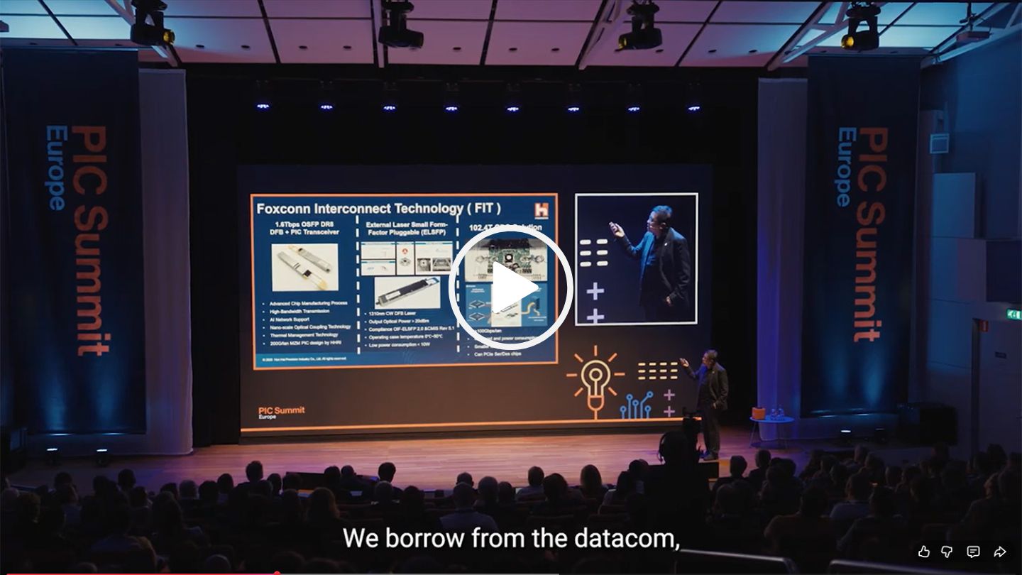
Have a look at the aftermovie of PIC Summit Europe 2025 to get an impression of what you can expect in 2026:
Why Attend?
|
Stay updated on speakers, programme & partnersStay up to date with all the latest news from PIC Summit Europe 2026 by signing up for the event mailinglist or by following our LinkedIn page. Don’t miss a single update about when registration is open, programme highlights, speaker announcements, and new partner reveals as they’re announced. |
| Follow on LinkedIN Email sign-up |
Scaling is not just about technology - it’s about strategy, execution, and collaboration. Whether you’re shaping the next generation of photonic chips or looking to integrate them into your solutions, PIC Summit Europe is where progress happens. Join us as we scale together in a dynamic world. Secure your spot today! |

LEADERS IN THE PHOTONIC CHIP INDUSTRY
Join start-ups, end-users, investors and academics at PIC Summit Europe
Photonic chip technology PIC Summit Europe is all about photonic chip technology and its applications. A technology that harnesses the power of light to create energy-efficient, faster, and more accurate microchips. Join and discover the latest developments. Rich programme & networking dinner The conference offers a rich programme with topics ranging from technology policy making, R&D, Heterogeneous Integration and industry applications like LiDAR and sensing. Next to this you can enjoy the many networking opportunities. |
Multiple side events & Tech Tour
PIC Summit Europe hosts multiple side events that will zoom in on current and pressing topics in the photonic chip industry such as talent attraction, startup funding, Quantum Photonics and roadmapping activities.
_Q2wKKqY.png) | PIC Industry Executive Forum | Monday 2 November 2026 (Invite only event)The PIC Industry Executive Forum 2025, an exclusive gathering of top European photonic integrated circuit (PIC) leaders, will be held on 3 November in Eindhoven. Timed just before PIC Summit Europe, the forum aims to shape the sector's strategic future amid major developments like the Chips Act 2.0, the next EU budget cycle, and the launch of PIXEurope - highlighting the urgent need for a unified, visionary industry voice. |
.png) | Tech Tour - Next Gen's IC | Wednesday 4 November 2026This side event is designed to foster strategic partnerships and investments, this programme will bring together high-impact companies, VCs, international investors, and industry experts. This is your chance to network face-to-face with the movers and shakers in the integrated circuits and next-gen computing sectors. |
 | Future of Integrated Photonics | Wednesday 4 November 2026The programme of this full-day side event aims to cover recent exciting findings from research labs together with scientific insights from companies (young and old) on how integrated photonics can be used to create innovative solutions. |
 | Technology Pavilion | Wednesday 4 November 2026Discover the latest innovations in integrated photonics at the Technology Pavilion. Dive into interactive demos, video animations, and project showcases from leading Dutch institutions and innovators. Connect with researchers, investors, and potential partners, and see breakthrough technologies in action. |
 | IPSR-I Autmn Meeting 2025 | Thursday 5 November 2026Global industry and R&D leaders unite to shape the future of photonics. Discover how the IPSR-I roadmap drives innovation in PIC technology by identifying system needs, solving manufacturing gaps, and accelerating application development. |
| Europe's most influential event in the photonic chip industry. Over 700 visitors from more than 20 countries. Organised and hosted by PhotonDelta - European Integrated Photonics Ecosystem. |
What to expect?
DAY 1: | DAY 2: |
| Features a curated mix of keynote speakers and panel discussions on a range of topics such as policy making, the future of chip design and semicon. | Presents industry keynotes exploring the state of the art of applications using photonic chips and a host of side events on topics such as startup funding, talent attraction and more. |
 60+ Expert speakers |  700+ Participants |
 |  |
| 20 | 40+ |
| Interactive Sessions | International partners |
PIC Summit Europe PartnersWe’re proud to collaborate with an incredible group of partners who help shape the future of PICs. Their contribution, expertise, and innovation in the industry play a key role in making this summit a leading platform for knowledge-sharing, collaboration, and business growth. |
 |
